Pins, balls and the package
You will learn
How the signals of your design reach the outside world.
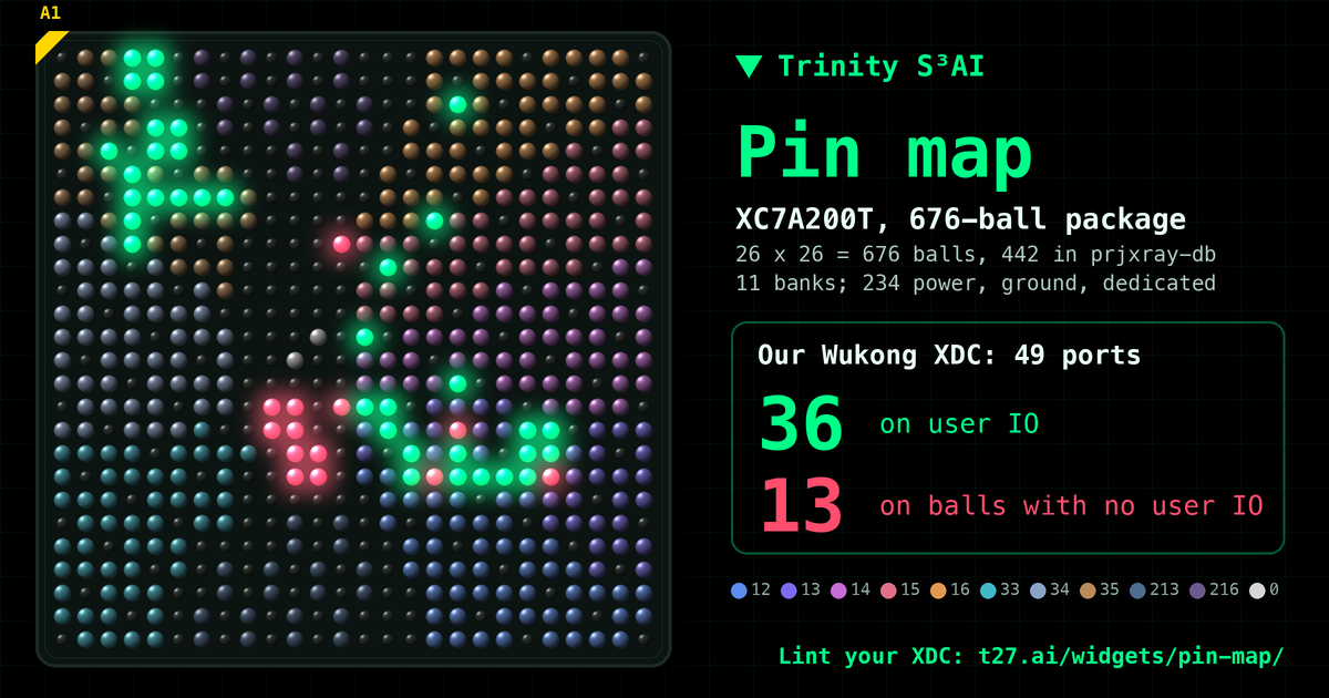
A chip sits in a package: the XC7A200T on our board has 676 solder balls under it. Some carry power or configuration and only some are user IO, grouped into banks with their own voltage. A constraints file (XDC) says which ball each signal of your design uses. Put a signal on a ball that is not user IO and the build fails, or worse, the board does not do what you think.
Try it
Search for a ball name like E3, then colour by pin type and find a ball that is not user IO.
All lessons
Module 1 · The chip
What an FPGA is, which chip we use, and how its pins meet the board.
Module 2 · Numbers in hardware
Bits, trits and number formats, and what arithmetic costs in logic.
Module 3 · Your t27 program
Write a spec, test it, and see why compiling is not the same as being right.
Module 4 · Inside t27c
How the compiler reads a spec and what it writes, including the native t27b.
Module 5 · From spec to hardware
The Verilog t27c writes, the cells it becomes, and what one LUT does.
Module 6 · Reading synthesis
What yosys reports about your design, and which warnings matter.
Module 7 · Place, route, timing
Where the cells land on the die, and whether the clock is met.
Module 8 · The bitstream
How a routed design becomes the bits the chip loads, with no Vivado.
Module 9 · On the board
Ask the chip who it is, load the bits, and check them.
Module 10 · Lab: our own research
A number format of our own, an honest scoreboard, and a model's tables multiplied on the board.