Modes: CPOL and CPHA
You will learn
What CPOL and CPHA mean, why there are four modes, and which one the spec configures.
CPOL picks the clock's idle level, CPHA picks which edge samples: four combinations, four modes, and devices that only speak one. The spec configures mode 0 -- SPI_CPOL 0, SPI_CPHA 0 -- and spi_mode_0_configuration is the test that pins it. The recording lowers the SPI spec to synthesizable Verilog.
Try it
In the recording, find the module ports the Verilog gives the SPI master; then in the spec frame find the mode-0 test and name what CPOL and CPHA each pick.
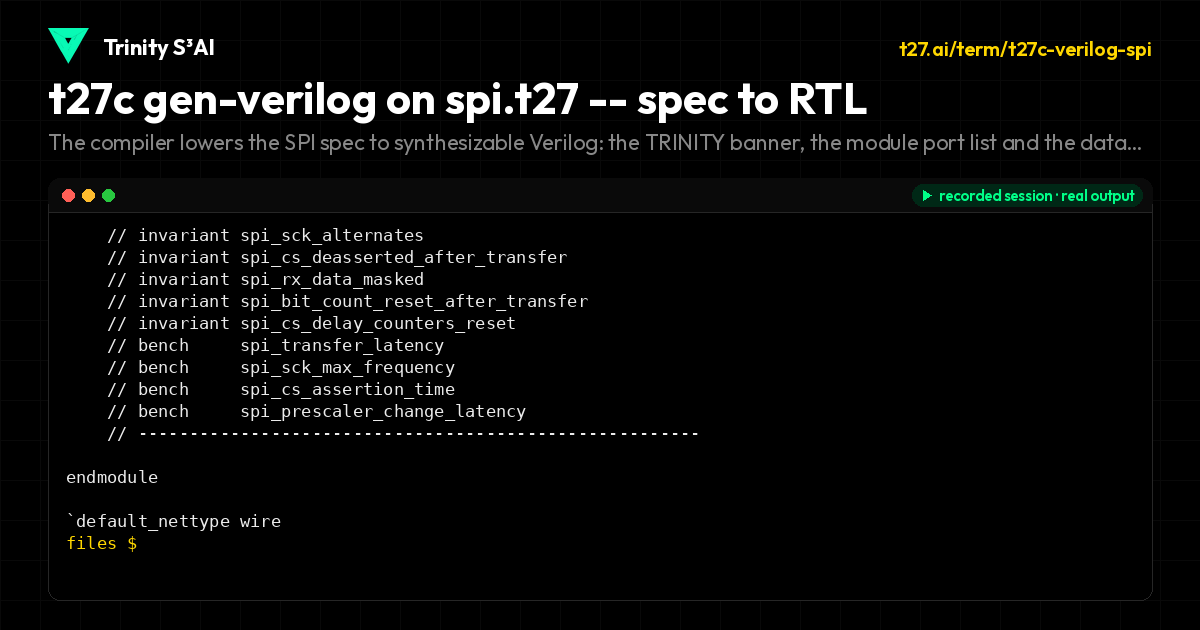
The compiler lowers the SPI spec to synthesizable Verilog: the TRINITY banner, the module port list and the datapath as wires.
specs/fpga/spi.t27
// SPDX-License-Identifier: Apache-2.0
// t27/specs/fpga/spi.t27
// SPI Master Specification for FPGA
// Mode 0: CPOL=0, CPHA=0 (SCK idle low, sample on rising edge)
// φ² + 1/φ² = 3 | TRINITY

module SPI_Master;
    // Import base types
    use base::types;

    // ═══════════════════════════════════════════════════════════════
    // 1. SPI Configuration
    // ═════════════════════════════════════════════════════════════════════════

    // System clock
    const CLK_FREQ : u32 = 50_000_000;    // 50 MHz

    // SPI Mode 0: CPOL=0, CPHA=0
    // CPOL (Clock Polarity): 0 = SCK idle low
    // CPHA (Clock Phase): 0 = Sample on first (rising) edge
    const SPI_CPOL : u8 = 0;
    const SPI_CPHA : u8 = 0;

    // SPI configuration
    const MAX_DATA_WIDTH : u8 = 32;       // Max bits per transfer
    const CS_ASSERT_DELAY : u32 = 100;     // CS to SCK delay (ns)
    const CS_DEASSERT_DELAY : u32 = 100;   // SCK to CS delay (ns)

    // SPI prescaler values (divides system clock)
    const PRESCALER_2 : u8 = 0;
    const PRESCALER_4 : u8 = 1;
    const PRESCALER_8 : u8 = 2;
    const PRESCALER_16 : u8 = 3;
    const PRESCALER_32 : u8 = 4;
    const PRESCALER_64 : u8 = 5;
    const PRESCALER_128 : u8 = 6;
    const PRESCALER_256 : u8 = 7;

    // ═══════════════════════════════════════════════════════════════
    // 2. SPI State Machine
    // ═════════════════════════════════════════════════════════════════════════

    // SPI states
    const SPI_IDLE : u8 = 0;
    const SPI_CS_ASSERT : u8 = 1;
    const SPI_TRANSFER : u8 = 2;
    const SPI_CS_DEASSERT : u8 = 3;

    // Transfer states
    const TX_BIT : u8 = 0;
    const RX_BIT : u8 = 1;
    const WAIT_EDGE : u8 = 2;

    // ═══════════════════════════════════════════════════════════════
    // 3. SPI Master Unit
    // ═════════════════════════════════════════════════════════════════════════

    // SPI master state
    struct SPI_Master_Unit {
        state : u8,                // Master state
        tx_state : u8,              // Transfer state
        cs_asserted : bool,          // Chip select state
        busy : bool,                // Transfer in progress

        // Transfer configuration
        prescaler : u8,            // Clock prescaler
        data_width : u8,            // Bits per transfer
        cs_mode : u8,              // CS mode (auto/manual)

        // Data registers
        tx_data : u32,              // Transmit data
        rx_data : u32,              // Receive data
        bit_count : u8,             // Bits transferred
        bit_counter : u32,          // Half-cycle counter

        // CS delay counters
        cs_assert_cnt : u32,        // CS assert delay
        cs_deassert_cnt : u32,      // CS deassert delay
    }

    // Default SPI unit
    var spi : SPI_Master_Unit = SPI_Master_Unit{
        .state = SPI_IDLE,
        .tx_state = TX_BIT,
        .cs_asserted = false,
        .busy = false,

        .prescaler = PRESCALER_16,  // Default: 16x prescaler
        .data_width = 8,           // Default: 8-bit transfers
        .cs_mode = 0,              // Auto CS

        .tx_data = 0,
        .rx_data = 0,
        .bit_count = 0,
        .bit_counter = 0,

        .cs_assert_cnt = 0,
        .cs_deassert_cnt = 0,
    };

    // spi_set_prescaler(psc: u8) → bool
    // Set SPI clock prescaler
    fn spi_set_prescaler(psc: u8) -> bool {
        if (psc > PRESCALER_256) {
            return false;
        }
        spi.prescaler = psc;
        return true;
    }

    // spi_get_prescaler_div() → u32
    // Get actual prescaler divider value
    fn spi_get_prescaler_div() -> u32 {
        // Was a `match` expression, which t27 has never parsed -- the whole
        // dispatch was silently DROPPED before the #1941 hardening (the fn
        // was an unimplemented stub). If-chain now.
        if (spi.prescaler == PRESCALER_2) { return 2; }
        if (spi.prescaler == PRESCALER_4) { return 4; }
        if (spi.prescaler == PRESCALER_8) { return 8; }
        if (spi.prescaler == PRESCALER_16) { return 16; }
        if (spi.prescaler == PRESCALER_32) { return 32; }
        if (spi.prescaler == PRESCALER_64) { return 64; }
        if (spi.prescaler == PRESCALER_128) { return 128; }
        if (spi.prescaler == PRESCALER_256) { return 256; }
        return 16;
    }

    // spi_get_sck_freq() → u32
    // Get SPI SCK frequency
    fn spi_get_sck_freq() -> u32 {
        return CLK_FREQ / spi_get_prescaler_div();
    }

    // spi_set_data_width(width: u8) → bool
    // Set data width (1-32 bits)
    fn spi_set_data_width(width: u8) -> bool {
        if (width == 0 || width > MAX_DATA_WIDTH) {
            return false;
        }
        spi.data_width = width;
        return true;
    }

    // spi_is_busy() → bool
    // Check if SPI is busy
    fn spi_is_busy() -> bool {
        return spi.busy;
    }

    // spi_transfer(data: u32) → bool
    // Start SPI transfer
    fn spi_transfer(data: u32) -> bool {
        if (spi.busy) {
            return false;
        }
        spi.tx_data = data;
        spi.rx_data = 0;
        spi.bit_count = 0;
        spi.bit_counter = 0;
        spi.state = SPI_CS_ASSERT;
        spi.busy = true;
        return true;
    }

    // spi_read_rx() → u32
    // Read received data (lower bits only)
    fn spi_read_rx() -> u32 {
        return spi.rx_data & ((1u32 << spi.data_width) - 1);
    }

    // spi_get_cs() → bool
    // Get CS line state
    fn spi_get_cs() -> bool {
        return spi.cs_asserted;
    }

    // spi_get_sck() → bool
    // Get SCK line state (Mode 0: idle low)
    fn spi_get_sck() -> bool {
        // In Mode 0: SCK is low in idle
        // Alternates during transfer
        // Was a `match` expression (never parsed; silently dropped pre-#1941).
        if (spi.tx_state == TX_BIT) { return false; }  // SCK low (setup)
        if (spi.tx_state == RX_BIT) { return true; }   // SCK high (sample)
        return SPI_CPOL == 0;
    }

    // spi_get_mosi() → bool
    // Get MOSI line state
    fn spi_get_mosi() -> bool {
        if (!spi.busy || spi.state != SPI_TRANSFER) {
            return false;  // Idle: MOSI low
        }
        return (spi.tx_data >> (spi.data_width - spi.bit_count - 1)) & 1 == 1;
    }

    // spi_tick() → void
    // Process one system clock cycle
    fn spi_tick() -> void {
        // Was a `match` statement (never parsed; the whole FSM tick was
        // silently dropped pre-#1941). If/else-if chain now.
        if (spi.state == SPI_CS_ASSERT) {
            spi.cs_assert_cnt = spi.cs_assert_cnt + 1;
            if (spi.cs_assert_cnt >= (CS_ASSERT_DELAY * CLK_FREQ / 1_000_000_000)) {
                spi.cs_assert_cnt = 0;
                spi.cs_asserted = true;
                spi.state = SPI_TRANSFER;
                spi.tx_state = TX_BIT;
            }
        } else if (spi.state == SPI_TRANSFER) {
            spi_transfer_bit();
        } else if (spi.state == SPI_CS_DEASSERT) {
            spi.cs_deassert_cnt = spi.cs_deassert_cnt + 1;
            if (spi.cs_deassert_cnt >= (CS_DEASSERT_DELAY * CLK_FREQ / 1_000_000_000)) {
                spi.cs_deassert_cnt = 0;
                spi.cs_asserted = false;
                spi.state = SPI_IDLE;
                spi.busy = false;
            }
        }
    }

    // spi_transfer_bit() → void
    // Transfer single bit
    fn spi_transfer_bit() -> void {
        const prescaler_div = spi_get_prescaler_div();
        spi.bit_counter = spi.bit_counter + 1;

        // Was a `match` statement (silently dropped pre-#1941).
        if (spi.tx_state == TX_BIT) {
            if (spi.bit_counter >= prescaler_div / 2) {
                spi.bit_counter = 0;
                spi.tx_state = RX_BIT;
            }
        } else if (spi.tx_state == RX_BIT) {
            if (spi.bit_counter >= prescaler_div / 2) {
                // Sample MISO 424 in spec-level simulation this is a placeholder;
                // Verilog emission reads the actual MISO input pin
                const miso_bit = false;
                spi.rx_data = (spi.rx_data << 1) | (if (miso_bit) { 1 } else { 0 });
                spi.bit_count = spi.bit_count + 1;
                spi.bit_counter = 0;

                if (spi.bit_count >= spi.data_width) {
                    spi.tx_state = WAIT_EDGE;
                } else {
                    spi.tx_state = TX_BIT;
                }
            }
        } else if (spi.tx_state == WAIT_EDGE) {
            if (spi.bit_counter >= prescaler_div / 2) {
                spi.bit_counter = 0;
                spi.state = SPI_CS_DEASSERT;
            }
        }
    }

    // ═══════════════════════════════════════════════════════════════════════════════════════════
    // TDD-Inside-Spec: Tests and Invariants for SPI_Master
    // ═══════════════════════════════════════════════════════════════════════════════════════════

    test spi_mode_0_configuration
        given cpol = SPI_CPOL
        and   cpha = SPI_CPHA
        then cpol == 0 and cpha == 0

    test spi_prescaler_16_default
        given psc = spi.prescaler
        then psc == PRESCALER_16

    test spi_set_prescaler_valid
        given result = spi_set_prescaler(PRESCALER_64)
        then result == true

    test spi_set_prescaler_invalid
        given result = spi_set_prescaler(99)
        then result == false

    test spi_prescaler_div_16
        given psc = PRESCALER_16
        and   div = spi_get_prescaler_div()
        then div == 16

    test spi_sck_freq_at_50MHz
        given freq = spi_get_sck_freq()
        and   div = spi_get_prescaler_div()
        then freq == CLK_FREQ / div

    test spi_set_data_width_8
        given result = spi_set_data_width(8)
        then result == true

    test spi_set_data_width_32
        given result = spi_set_data_width(32)
        then result == true

    test spi_set_data_width_invalid
        given result = spi_set_data_width(0)
        then result == false

    test spi_initially_not_busy
        given busy = spi_is_busy()
        then busy == false

    test spi_transfer_when_ready
        given result = spi_transfer(0xAA)
        then result == true

    test spi_transfer_when_busy
        given spi_transfer(0x55)
        and   result = spi_transfer(0xAA)
        then result == false

    test spi_cs_idle_high
        given cs = spi_get_cs()
        then cs == false

    test spi_sck_idle_low
        given sck = spi_get_sck()
        then sck == false  // Mode 0: idle low

    test spi_max_data_width_32
        given max = MAX_DATA_WIDTH
        then max == 32

    test spi_prescaler_range
        given min_psc = PRESCALER_2
        and   max_psc = PRESCALER_256
        then min_psc == 0 and max_psc == 7

    test spi_cs_delays_defined
        given assert_delay = CS_ASSERT_DELAY
        and   deassert_delay = CS_DEASSERT_DELAY
        then assert_delay == 100 and deassert_delay == 100

    invariant spi_mode_0_constant
        assert SPI_CPOL == 0 and SPI_CPHA == 0

    invariant spi_states_valid
        given state = spi.state
        assert state == SPI_IDLE or state == SPI_CS_ASSERT or state == SPI_TRANSFER or state == SPI_CS_DEASSERT

    invariant spi_tx_states_valid
        given tx_state = spi.tx_state
        assert tx_state == TX_BIT or tx_state == RX_BIT or tx_state == WAIT_EDGE

    invariant spi_prescaler_divides_clock
        given freq = spi_get_sck_freq()
        assert CLK_FREQ % freq == 0

    invariant spi_data_width_bounds
        assert spi.data_width > 0 and spi.data_width <= MAX_DATA_WIDTH

    invariant spi_busy_implies_cs_asserted
        assert spi.busy == false or spi.cs_asserted or spi.state == SPI_CS_ASSERT

    invariant spi_busy_only_in_transfer
        assert spi.busy == false or spi.state == SPI_CS_ASSERT or spi.state == SPI_TRANSFER or spi.state == SPI_CS_DEASSERT

    invariant spi_sck_alternates
        given old_sck = spi_get_sck()
        when spi.state == SPI_TRANSFER and spi.tx_state == TX_BIT
        and   spi.tx_state = RX_BIT
        and   new_sck = spi_get_sck()
        then old_sck != new_sck

    invariant spi_cs_deasserted_after_transfer
        given spi.data_width = 8
        and   spi_transfer(0xAA)
        then spi.state == SPI_CS_DEASSERT or spi.state == SPI_IDLE

    invariant spi_rx_data_masked
        given spi.data_width = 8
        and   spi.tx_data = 0xAA55AA55
        and   rx = spi_read_rx()
        then rx == rx & 0xFF

    invariant spi_bit_count_reset_after_transfer
        given spi.data_width = 8
        and   spi.bit_count = 8
        when spi.state == SPI_CS_DEASSERT and spi.state == SPI_IDLE
        and   spi.busy == false
        then spi.bit_count == 0

    invariant spi_cs_delay_counters_reset
        given spi.state == SPI_IDLE
        then spi.cs_assert_cnt == 0 and spi.cs_deassert_cnt == 0

    bench spi_transfer_latency
        measure: nanoseconds to complete 8-bit transfer
        target: < 2000ns  // 8 bits * 2 * prescaler / 50MHz

    bench spi_sck_max_frequency
        given spi_set_prescaler(PRESCALER_2)
        and   freq = spi_get_sck_freq()
        then freq == 25_000_000  // 50MHz / 2

    // CS_ASSERT_DELAY (100ns) plus margin
    bench spi_cs_assertion_time
        measure: nanoseconds for CS assertion
        target: < 150ns

    bench spi_prescaler_change_latency
        measure: nanoseconds to spi_set_prescaler(PRESCALER_32)
        target: < 100ns
All lessons
Module 1 · What a bus is
Why a bus exists at all: a conversation on wires, framed and addressed, and who is allowed to talk.
Module 2 · UART
The two-wire bus with no clock: the frame, the divisor that sets the rate, and the status a driver polls.
Module 3 · SPI
The clocked conversation: four modes, a prescaler ladder, and a chip select per servant.
Module 4 · APB
The register bus: PSEL and PENABLE, strobes and wait states, and how many address bits a peripheral count costs.
Module 5 · AXI4
The five channels: address, data and response in both directions, lite or full, bursts and IDs.
Module 6 · Memory
What sits on the far side of every bus: memory maps, port kinds, and latency that a wait state must cover.
Module 7 · Bridges
Why designs grow more than one bus, and the packet bridge that moves work between them.
Module 8 · Ethernet
Frames, the frame check sequence, RGMII timing, and the pre-registered steps of a real bring-up.
Module 9 · The bench
The discipline that guards real hardware: who holds the IO, taking and giving the lock, and what runs next.