RGMII timing
You will learn
What RGMII timing demands of a double-data-rate nibble, and what the spec asserts of it.
RGMII moves a nibble per clock edge, both edges: double data rate at 125 MHz for gigabit, and a single-data-rate downshift for 10 and 100. The spec of this lesson, written for this course, carries the timing arithmetic and its assumptions in the header. The recording runs t27c on it.
Try it
In the recording, watch the run; then in the spec frame find the DDR rate and what the spec says of the 10 and 100 downshift.
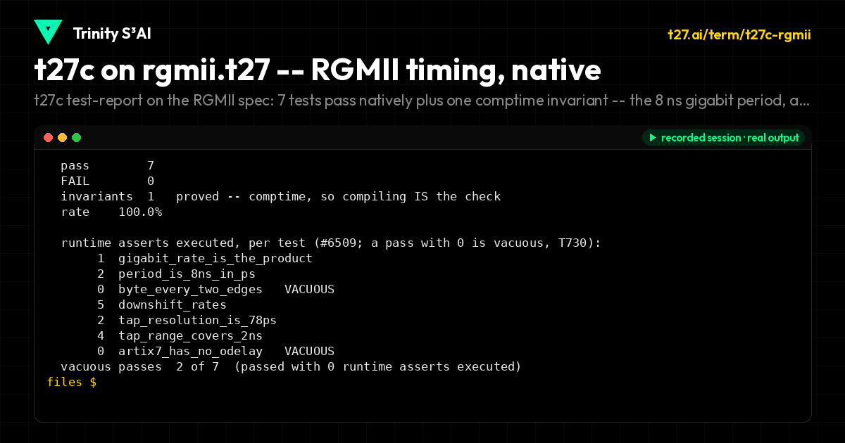
t27c test-report on the RGMII spec: 7 tests pass natively plus one comptime invariant -- the 8 ns gigabit period, a nibble on both edges, the 78 ps tap ladder.
specs/fpga/rgmii.t27
// SPDX-License-Identifier: Apache-2.0
; rgmii.t27 -- RGMII v2.0 timing arithmetic, as one spec.
; The reduced gigabit media-independent interface: 4 data bits, both clock
; edges, 125 MHz -- 1000 Mbps over 12 pins. This spec owns the arithmetic a
; design applies when it reasons about RGMII: periods, bit times, downshift
; rates, and how many IDELAY taps a skew budget needs.
; ----
; SOURCE:
;   RGMII specification v2.0 (HP, April 2002)   DDR data, 125 MHz TXC,
;       internal-delay option (RGMII-ID), 10/100 downshift
;   Xilinx UG471 (7 Series SelectIO)            IDELAYE2 tap resolution
;       = 1 / (32 x 2 x f_REF): 78 ps at the 200 MHz reference, 31 taps
;   Xilinx UG471                                  ODELAYE2 exists in HP
;       banks only; Artix-7 has HR banks, so no output delay element
; ORACLE: the constants are cited above; every other number in this file is
; derived by the test blocks below from those constants -- no figure is
; transcribed from memory. (U64 widening for the 1e12 ps-per-second product
; follows the simulator.t27 idiom.)
; ----
; THEORETICAL: no RGMII board measurement backs this spec yet (no rgmii run
; exists on the bench -- checked 2026-10-08). Course pages built on it must
; say the numbers are theoretical until a board run lands. Board PHYs differ
; (Wukong xc7a200tfgg676 vs AX7203 xc7a200tfbg484); name the board.
; ----
; Course use: trinity buses-and-peripherals module 8, lessons rgmii and
; idelay-and-odelay (gHashTag/trinity#1484).

module fpga_rgmii;

; --- The interface, straight from the spec sheet ---------------------------

pub const RGMII_CLOCK_HZ   : u32 = 125_000_000;
; one nibble per DDR phase
pub const RGMII_DATA_BITS  : u32 = 4;
; data on both clock edges
pub const RGMII_EDGES      : u32 = 2;
pub const RGMII_IDEAL_MBPS : u32 = 1000;

; 10/100 downshift: same pins, slower clock (RGMII v2.0 1000/100/10)
pub const RGMII_100_HZ     : u32 = 25_000_000;
pub const RGMII_10_HZ      : u32 = 2_500_000;

; --- Xilinx 7-series delay elements (UG471) --------------------------------

pub const IDELAY_REF_HZ    : u32 = 200_000_000;
pub const IDELAY_TAPS      : u32 = 31;
; Artix-7 = HR banks only (UG471)
pub const HAVE_ODELAY      : bool = false;

; ps per tap = 1e12 / (32 * 2 * f_REF). The 1e12 product needs u64 (the
; simulator.t27 ns arithmetic hits the same wall); the result fits u32.
pub fn tap_resolution_ps(ref_hz : u32) u32 {
    return ((1_000_000_000_000 as u64) / ((32 * 2) as u64 * (ref_hz as u64))) as u32;
}

; tap_resolution_ps(200 MHz), asserted below
pub const IDELAY_RESOLUTION_PS : u32 = 78;

pub fn clock_period_ps(hz : u32) u32 {
    return ((1_000_000_000_000 as u64) / (hz as u64)) as u32;
}

; Gigabit clocks run DDR (both edges); the 10/100 downshift drops to SDR --
; rising edge only -- or 25 MHz DDR would carry 200 Mbps, not 100.
pub fn mbps(clock_hz : u32, edges : u32) u32 {
    return (RGMII_DATA_BITS * edges * clock_hz) / 1_000_000;
}

pub fn taps_for_shift_ps(shift_ps : u32) u32 {
    return (shift_ps + IDELAY_RESOLUTION_PS - 1) / IDELAY_RESOLUTION_PS;
}

test gigabit_rate_is_the_product {
    assert mbps(RGMII_CLOCK_HZ, RGMII_EDGES) == RGMII_IDEAL_MBPS;
}

test period_is_8ns_in_ps {
    assert clock_period_ps(RGMII_CLOCK_HZ) == 8000;
    assert clock_period_ps(RGMII_CLOCK_HZ) / RGMII_EDGES == 4000;
}

test byte_every_two_edges {
    const bytes_per_s = (RGMII_IDEAL_MBPS * 1_000_000) / 8;
    assert bytes_per_s == 125_000_000;
}

; 100 Mbps = 25 MHz SDR, 10 Mbps = 2.5 MHz SDR (RGMII v2.0)
test downshift_rates {
    assert mbps(RGMII_100_HZ, 1) == 100;
    assert mbps(RGMII_10_HZ, 1) == 10;
    assert mbps(RGMII_100_HZ, 2) == 200;
    assert clock_period_ps(RGMII_100_HZ) == 40_000;
    assert clock_period_ps(RGMII_10_HZ) == 400_000;
}

test tap_resolution_is_78ps {
    assert tap_resolution_ps(IDELAY_REF_HZ) == 78;
    assert IDELAY_RESOLUTION_PS == tap_resolution_ps(IDELAY_REF_HZ);
}

test tap_range_covers_2ns {
    const range_ps = IDELAY_TAPS * IDELAY_RESOLUTION_PS;
    assert range_ps == 2418;
    assert taps_for_shift_ps(2000) == 26;
    assert taps_for_shift_ps(2000) <= IDELAY_TAPS;
    assert taps_for_shift_ps(4000) == 52;
    assert taps_for_shift_ps(4000) > IDELAY_TAPS;
}

test artix7_has_no_odelay {
    assert HAVE_ODELAY == false;
}

invariant rate_matches_clock {
    mbps(RGMII_CLOCK_HZ, RGMII_EDGES) == (RGMII_DATA_BITS * RGMII_EDGES * RGMII_CLOCK_HZ) / 1_000_000
}
All lessons
Module 1 · What a bus is
Why a bus exists at all: a conversation on wires, framed and addressed, and who is allowed to talk.
Module 2 · UART
The two-wire bus with no clock: the frame, the divisor that sets the rate, and the status a driver polls.
Module 3 · SPI
The clocked conversation: four modes, a prescaler ladder, and a chip select per servant.
Module 4 · APB
The register bus: PSEL and PENABLE, strobes and wait states, and how many address bits a peripheral count costs.
Module 5 · AXI4
The five channels: address, data and response in both directions, lite or full, bursts and IDs.
Module 6 · Memory
What sits on the far side of every bus: memory maps, port kinds, and latency that a wait state must cover.
Module 7 · Bridges
Why designs grow more than one bus, and the packet bridge that moves work between them.
Module 8 · Ethernet
Frames, the frame check sequence, RGMII timing, and the pre-registered steps of a real bring-up.
Module 9 · The bench
The discipline that guards real hardware: who holds the IO, taking and giving the lock, and what runs next.